Together We Can Do It!

This page is ad-free, instead of donating to me please consider supporting the Ukraine.

United24.ua

Home About my QRZ.com YouTube

Tuned 433 MHz small signal amplifier

Description:

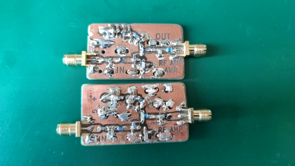
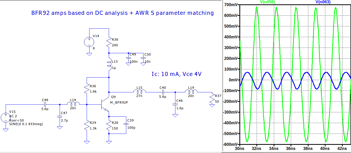
In this small project, I wanted to design an RF amplifier from scratch. Of course, the simplest solution is to use an off-the-shelf MMIC that implements the bias network and impedance matching, but that offers a very limited learning experience. Therefore, I decided to design a single-stage class A amplifier around a popular BFR92 VHF/UHF bipolar transistor.

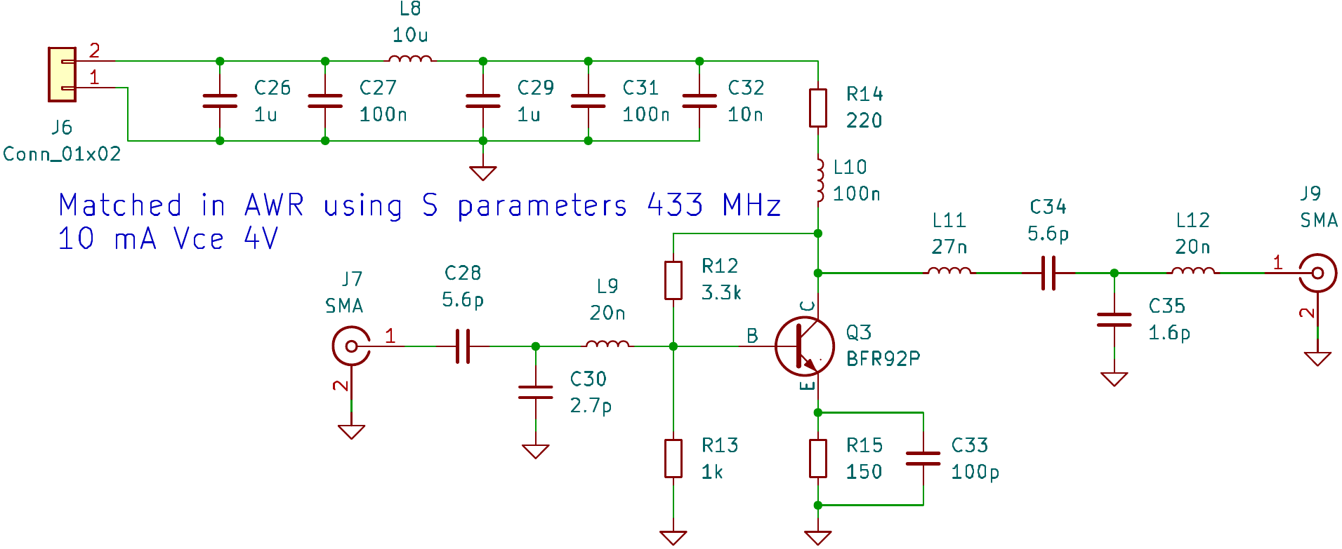
The center design frequency was chosen as 433 MHz because I expect this amplifier to cover both the ISM band and the 70 cm amateur radio band. Additionally, at the time of designing this amplifier, I was also working on two projects that could make use of an amplifier tuned around that frequency. Since the wavelength is much longer than any SMD component, the lumped model and discrete LC components were used. It was also expected that the LC values would be within the range of possible SMD components (not smaller than 1 pF for example). I wanted to achieve more than 16 dB of gain, something that is possible with a single BFR92 transistor. What was more important in this design was minimal reflection from the input and the output. This is because I wanted to use this amplifier before a mixer or after an intermediate frequency filter. Mixers can be sensitive to back reflection, so good return loss is always a plus.

Design of the amplifier

  • Chosing transistor and DC operating point. TThere is a lot to be said about this point, but I chose the BFR92 because of its low price and relatively high transition frequency. The collector current was chosen as 15 mA since it guarantees a higher transition frequency and slightly higher gain. Many of the characteristics in the datasheet table are also given for 15 mA, so it is a good starting point. However, for lower noise, a value of 10 mA might be a better choice. If you need to design an LNA, keep that in mind.

  • DC network design I have chosen the values of the biasing network to achieve a collector current of 15 mA and a collector-to-emitter voltage of 6 V. With a supply voltage (Vcc) of 10 V, this will set the quiescent point roughly in the middle. An important aspect of Vce is that it also impacts the scattering parameters of the transistor in your two-port network. If you don't want to measure the .s2p files yourself in a custom test fixture, check if your transistor has ready simulation models or example .s2p files. In my case, Infineon had a very handy Spice model Infineon had a very handy Spice model (I have used it for DC simulation) and a sweep of S parameters in .s2p files for different values of Ic and Vce (I have used those for impedance matching).

  • Designing input and output matching networks I am skipping a point in this project that might be crucial in more professional designs: stability conditions and stability circles. Generally, it might turn out that your design will end up in a part of the Smith chart where the amplifier is unstable under certain conditions, leading to oscillations that can also occur outside of your desired spectrum.
    During this project, I had access to AWR Designer, which I used to design the impedance matching. You can also use LTSpice to measure complex impedance and a Smith chart program (I recommend Smith 4.1) to design matching networks, but it is more difficult to iterate through designs in that way since changes in the input network will affect the output matching to some extent, and vice versa.
    In AWR Designer, I imported the S parameters using the NPORT_F element (you can change its icon to look like a BJT in CE configuration) and then used the filter design tool to create an initial input network based on port 1. After placing components on the schematic, I repeated the procedure with the filter design tool for impedance matching, but looking from port 2. After that, the tuner tool can be used to adjust the two networks for optimal return loss. Again, my main concern was obtaining the best return loss and a working amplifier. For a better noise figure or stable gain, you might want to do more math. The filter design tool is very useful here because it allows you to choose different topologies of matching with various characteristics and orders.

  • Moving the design to PCB I then used KiCad to create a schematic and PCB layout for the amplifier. For such small projects with relatively wide traces, I fabricate the boards at home. I don't use microstrip lines or any controlled impedance traces in this design because the wavelength is relatively long compared to the PCB. Of course, keeping the design small is still important. I decided to use 0805 SMD components for ease of soldering and prototyping.

  • Measurement This is my favorite part. First, the DC operating point had to be checked. After applying 10 V at the DC input, the total current draw was 15.7 mA. Subtracting the current flowing through the bias network, the collector current was measured to be 14.1 mA. This is a little bit smaller than simulated (15 mA), but should be good enough. The collector-emitter voltage was measured at 6.17 V, which is very close to the expected value. It can be concluded that the Spice model provided by Infineon works well for DC.
    During this DC measurement, the ports of the amplifier were terminated in 50 Ohm SMA loads.
    Next, I used the Lite VNA with a 6 dB attenuator at port 1 and a 10 dB attenuator at port 2 to measure the scattering parameters of the amplifier. Before that, the VNA was calibrated with the attenuators attached. This limits the dynamic range of the instrument, so the Nano VNA or Lite VNA 64 is not the best here, but it was good enough.

Results

schematic BFR92
Schematic of the amplifier
Real amplifier
Measurement of real amplifier
Smithchart
Smith chart of the input and output return loss of real amplifier

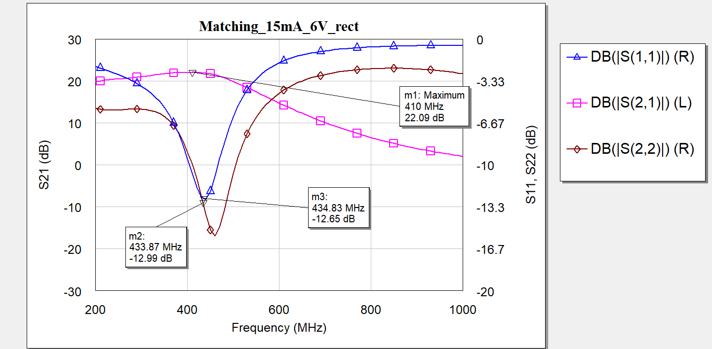
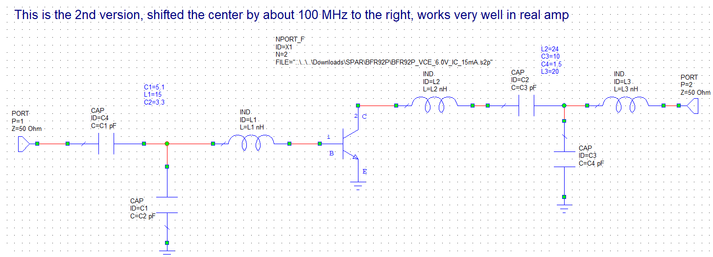
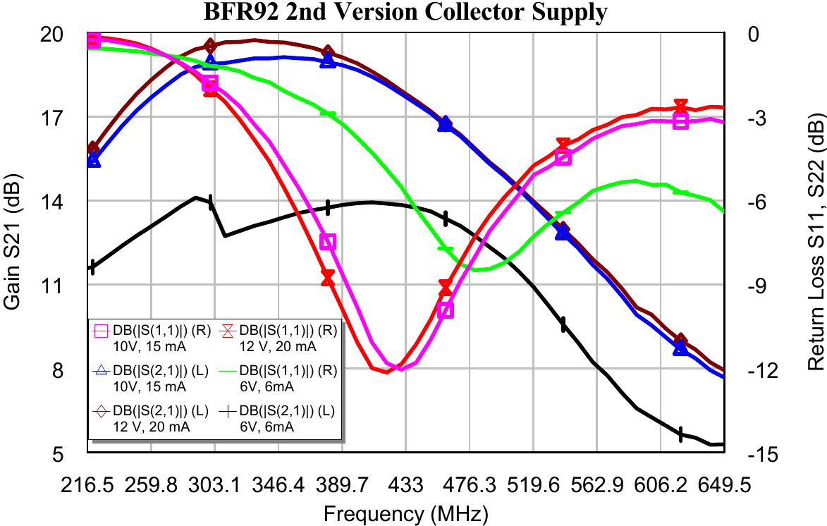
The first version of the amplifier had a characteristics shifted to a lower frequency. By calculating the difference and retuning the amplifier in AWR by said difference, I made a second version. The results in the above figures come from that second version of the retuned amplifier. As can be seen, the return loss has its global minimum almost exactly at the desired 433 MHz. The magnitude of the return loss is also very good, -12 dB for the input and -16.5 dB for the output. The achieved gain is also higher than the desired minimum; here, 17.7 dB was obtained instead of 16 dB.

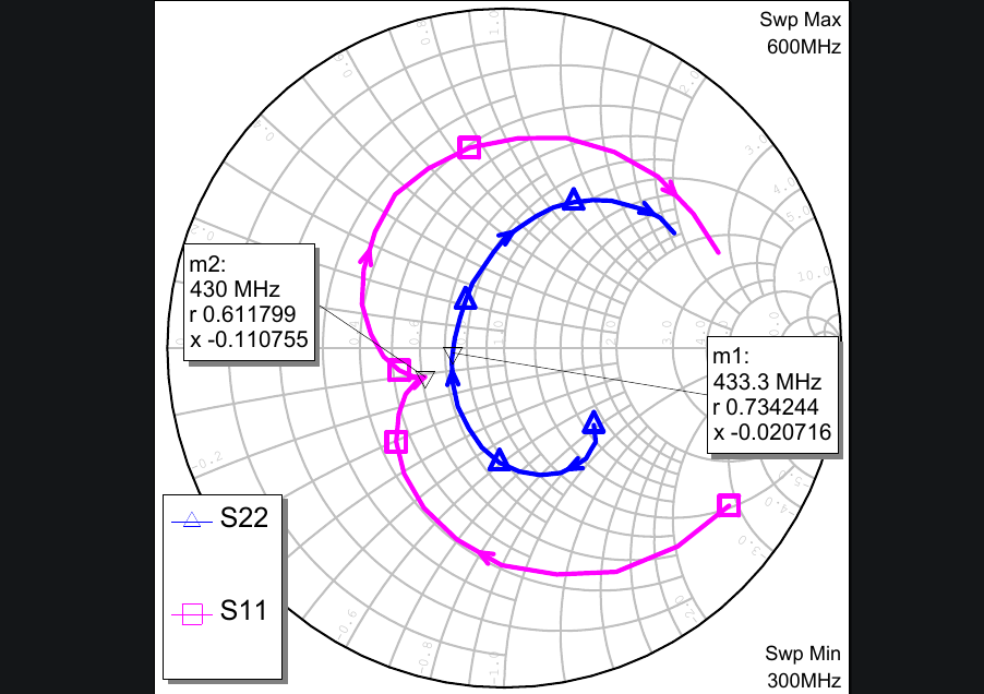
One interesting observation is that the maximal gain (MSG - maximal stable gain) occurs at a different point than the minimum return loss. This is normal behavior that in a more complex design would be presented on a Smith chart using gain and stability circles. In such a Smith chart, the rotation does not indicate a change of the frequency axis; the circles indicate a boundary where certain conditions are maintained, and the plot is made for a single frequency point.
The used .s2p file did not include noise parameters, so I was not able to simulate noise circles for this circuit. However, using the gain method and a spectrum analyzer, I measured a noise figure of 3.68 dB. Not great by any means, but it is a good parameter to know. Lowering Ic and conducting a more in-depth analysis of noise circles could reveal a design with potentially worse return loss but better NF. In RF, you rarely get something for free; some compromises usually have to be made.

In conclusion, if you want a sure way of getting a working LNA, the MMIC is most likely the best choice if you value your sanity and time. If you want to learn something, then designing a BJT RF amplifier is a good challenge. I highly recommend designing at least one amplifier like this if you are an amateur radio operator or if you want to construct your own RF devices in the future.

I have also verified that the amplifier offers the best performance for the 10 V input voltage by performing a simple push/pull effect measurement, which shows the effect of supply voltage on S21, S11, and S22. It can be observed that the input voltage affects the S parameters, as proper matching is achieved for 10 V and 12 V, with only 10 V resulting in a global minimum exactly at 433 MHz.
In the future, I would like to revisit this project and measure its linearity in terms of IP3 and IMD3. Currently, I don't have a signal generator that can control the output power at that frequency, oh well...

Spice
LTspice simulation
AWR
AWR Designer schematic of retuned version
push pull effect
Snith chart of the input and output return loss of real amplifier

Radios

Contact me

sp6gk 'at' protonmail.com

Restored tube radio

Here is demonstration of a restored radio from 1938.

Band conditions

Check out my RF amplifiers with distributed matching networks

2.4 GHz PA

Almost assembled fully home made 2.4 GHz power amplifier on LDMOS transistor.


2400 MHz hairpin v1

1.25 GHz small signal amplifier with open stub matching. Active element is BFP420 BJT.


Flag counter

Flag Counter

My QO-100 Satelite dish

Satelite dish

My 120 cm prime focus dish. For now in the feed I have the Bullseye LNB. Thanks to my home made bias Tee and polarization controller I can receive the QO-100 satelite just fine on the RTL-SDR. Now I am working on upconverter and 2.4 GHz PA for the uplink.